DC Protection and Time Delay Circuit for Amplifiers
Description
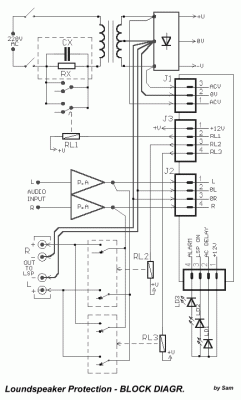
An exceptionally useful circuit for final amplifiers, as well as in various applications requiring a time delay and protection against DC. This particular circuit combines several essential operations: [1] A smooth transition of AC line voltage to the power supply transformers via RL1 and resistance Rx with a 1-second delay. (See block diagram). [2] Delaying the connection of final amplifier output to headphones, preventing noise from the charging or discharging of capacitors in the power supply from being passed through. Simultaneously, it ensures continuous DC voltage at the amplifier's output. If everything functions correctly, the amplifiers connect to the speakers. During the operation of the amplifiers, there is constant monitoring of DC voltage; if a problem occurs (e.g., an open transistor in the final stage), the power supply voltage bypasses to the loudspeakers. [3] An error signal that is indicated both visually by LD3 (can flash) and audibly with BZ.
Another feature not commonly found in proportional circuits, is the inclusion of a second relay (RL3) with parallel contacts to RL2, which helps connect the speakers after the main relay RL2 has partially closed. The addition of this relay was motivated by frequent degradation of RL2’s contacts due to the electric arcs generated when it opens and closes. This results in a spectrum of frequencies and degrades sound quality due to the high resistance developed across the contacts. Adding another set of contacts that close simultaneously with those of RL2 mitigates this issue, keeping the contacts clean and reducing potential differences that can lead to their degradation.
How it works
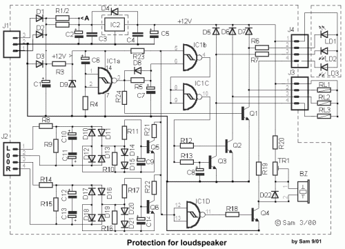
The circuit is supplied from an AC line through J1. The voltage could be derived from a separate 2x12V transformer (the material prices I provide are for this configuration), or from existing 12V coils in the power amplifier's MT, or if not available, from the main supply transformers of the final amplifier. Always adjust resistances R1/2 and R3 proportionally to the supplied voltage according to Ohm’s law and desired voltage drop (R=V/i). The point A before IC2 should have a voltage greater than +15V at 200mA, as this powers all relays and LEDs. The rest of the circuit is powered by R3/D9. When the amplifier receives network voltage via J1, C6 charges through R4; the input to IC1a (H) exit (L) Q1-RL1 remains open. As the first MT in the power supply intervenes, RX ensures a smooth transition of the main MT to the network voltage, preventing fuse burnout, especially with high-power supplies. After 1 second of C6 charging, its negative pole reaches 0V; IC1A’s input becomes 0V (L), causing Q1 to close RL1, shorting Rx and applying full network voltage to the main MT. Simultaneously, LD1 turns on via R5 slowly charging C7 (~5 seconds). Once C8 is charged (~2 seconds) through R13, conductance of Q3 opens RL3’s contacts along with those of RL2. The circuit operates fully. Disconnecting the network line causes a rapid shutdown of all supplies, quickly cutting off speakers. If DC voltage appears at J2/1 and J2/4 inputs, the circuits for detecting DC activate, causing Q5 or Q6 to conduct, leading IC1b’s pin 5 to 0V (L). This results in IC1c’s exit becoming (H), turning off transistors Q2-3 and opening RL2-3, disconnecting speakers from amplifier output until the cause of DC is resolved. The same time, IC1D’s exit becomes (H), causing Q4 to conduct, BZ sounds, and LD3 signals an error. The intensity of BZ sound can be adjusted using TR1; it can also be muted if no error signal is needed. Adjusting times involves changing capacitors C7-8 with different capacities, while R1-2 should be kept away from the PCB due to potential heat. IC2 needs a heatsink when entry voltage exceeds +15V. Care must be taken for resistance RX/CX and RL1 contacts due to network voltage danger (DANGER OF ELECTROCUTION). Insulation is crucial here. The quality of all relays should be very good and from known manufacturers.
Circuit diagram
Part list
- R1-2=See text*
- R3=470R 1W*see text
- R4-5= 1M
- R6-7= 1K
- R8-14= 15K
- R9-15= 56K
- R10-16= 56K
- R11-17= 10K
- R12-13= 39K
- R18= 39K
- R19= 1K2
- R20= 1K
- R21-22= 3K9
- R23= 22K
- R24= 39K
- RX= 47R 10W
- C1= 220uF 63V
- C2-5= 47uF 63V
- C3-4=100nF
- C6= 1uF 25V
- C7= 4.7uF 25V
- C8= 470uF 16V
- C9-14= 22uF 16V
- C10-13= 33uF 63V
- CX= 33nF 630V
- IC1= 4093 CMOS
- IC2= 7812T
- Q1-4= BD679
- Q5-6= BC550C
- D1-4= 1N4007
- D5-8= 1N4148
- D9=12V 1.2W Zener
- D10-22= 1N4148
- LD1-2= LED
- LD3= Flash Led [RED]
- BZ= BUZZER 12V
- J1-4= Connectors
- TR1= 10K Trimmer
- RL1-3= 12V 2X2(10A) RELAY

