Protect Voltage Regulators: Simple Circuit for 60V Input
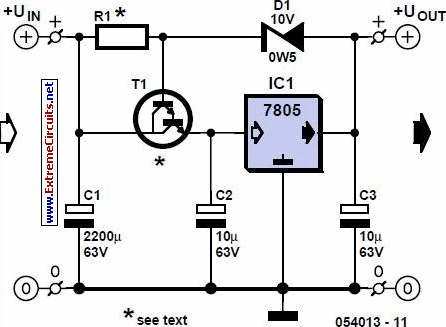
Circuit diagram
Voltage regulator circuits often possess a defined upper limit on the allowable input voltage – typically around 35 V for fixed-output models. Adjustable regulators also have a maximum voltage specification, generally between the input and output, frequently 40 V. Therefore, the input voltage must be constrained to this level during fault conditions when the output is shorted.
This circuit demonstrates a method for utilizing these regulators in situations involving elevated input voltages. Although the solution incorporates an additional three components, it’s straightforward and can be constructed using readily available parts. The voltage across the regulator is restricted by the combination of T1 and zener diode D1 to a value that permits proper operation with loads up to its maximum rated capacity. R1 furnishes sufficient operating current for D1 and the bias current for T1.
Employing a Darlington type for T1 is advisable to maintain a reasonably high value for R1. The current flowing through D1 is only 10 mA with a 60 V input voltage. Naturally, we assessed the circuit’s behavior when no load is connected. Remarkably, the nominal output voltage of 5.02 V increased to only 5.10 V (with a 60-V input voltage). During our experiments, we utilized a BDV65B for T1 and a value of 4.7 kO for R1.
To guarantee that the circuit is entirely short-circuit resistant with a 60 V input voltage, a transistor is required that remains within its safe operating area at the maximum input voltage combined with the short-circuit current of the regulator – which may exceed 2 A. The BDV65B and TIP142 do not satisfy this requirement. The maximum voltage for the BDV65B is actually 40 V, and for the TIP142 is 50 V. If the transistor fails, the regulator will also fail. This was verified experimentally.
Adding SOA protection for T1 is one possibility, but it essentially protects the protection. Alternatively, the requirements can be relaxed. To achieve this, R1 must supply sufficient current to ensure that T1 receives enough current during a short circuit to keep the voltage across T1 lower, although this makes little practical difference and also increases the minimum load. Furthermore, it should be evident that adequate cooling for T1 and IC1 must be provided according to the load.
Ripple suppression is only marginally affected by the protection circuit, since the input is already well stabilized by T1, but the current through D1 does flow through the output. The presence of C2 must also be taken into account. In this circuit, with an adjustable voltage regulator such as the LM317 and an output voltage greater than 40 V, C2 will cause the voltage to be briefly higher than 40 V during a short circuit, which can also damage the IC. In this case, a different solution or a different type of voltage regulator must be sought.
The LM317 is a three-terminal adjustable voltage regulator that allows precise control of the output voltage. It operates with a fixed current of 50 µA, providing a stable output even with varying loads. The LM317 is a widely used IC offering versatility in a variety of applications, from power supplies to instrumentation. Its versatility and relatively low cost make it a popular choice for many circuit designs. The LM317 is a monolithic integrated circuit that operates as a voltage regulator, allowing for precise output voltage control. It features three terminals: Input, Output, and Adjust, enabling fine-tuning of the output voltage based on the external potentiometer. This integrated design ensures robust performance and reliability.
circuit from http://www.extremecircuits.net/2010/05/protection-for-voltage-regulators.html
