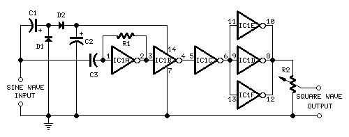
Self-Powered Sine to Square Wave Converter Diagram
Transforms sine waves into square waves without requiring an external power supply
It serves as a valuable testing instrument specifically for audio applications
Circuit Diagram
Components:
- R1 1M 1/4W Resistor
- R2 100K Linear Potentiometer
- C1, C2 100µF 25V Electrolytic Capacitors
- C3 10nF 63V Polyester Capacitor
- D1, D2 1N4148 75V 150mA Diodes
- IC1 4069 Hex Inverter IC
Device Objective:
This circuit is designed to yield effective square waves, converting a sine wave obtained from an existing generator. A key attribute is the absence of the need for an external power source; therefore, it can be readily connected between a sine wave generator and the device being tested. The incoming sine wave is fed into a voltage multiplier constructed from C1, C2, D1 & D2, which then supplies power to IC1. IC1’s amplifier boosts the initial sine wave, while other inverters within IC1 generate a squared signal, producing an output square wave with a balanced mark/space ratio and well-defined rise and fall times across a frequency range of 20Hz to 20KHz.
Notes:
- Optimal performance is achieved with an input sine wave amplitude of at least 1V RMS.
- The output square wave amplitude is correlated with the input amplitude.
- The minimum sine wave input amplitude needed for satisfactory performance: 750mV RMS.
- Output square wave amplitude with a 1V RMS input: 3V peak to peak, when R2 is set at its maximum value.
- The minimal output square wave amplitude: 2V peak to peak, with R2 set at maximum.
- Replacing the two silicon diodes with germanium types (such as AA118, AA119) allows for a reduction in the minimum input threshold.
This circuit received £50 and was featured in the “Circuit Ideas” section of ELECTRONICS WORLD, February 2000 issue, page 135.
IC1 - 4069 Hex Inverter IC
The 4069 is a versatile hex inverter integrated circuit commonly utilized in a variety of analog and digital circuits. This particular IC is a bipolar junction transistor (BJT) based inverter, meaning that each input signal is inverted by the corresponding transistor. Its six outputs are configured to invert the corresponding input signal, offering a convenient solution for numerous circuit designs. With a low supply voltage requirement, the 4069 is a cost-effective choice for building complex logic circuits and signal processing applications. It is a popular selection for students and hobbyists due to its ease of use and readily available datasheets. The IC operates with a supply voltage of approximately 15V, allowing it to function reliably in a range of circuit designs. The pinout of the 4069 IC includes six outputs, which are typically labeled as QB, QC, QA, QB1, QB2, QB3, and QB4. Each output is a BJT that performs the inversion function. The IC is suitable for a wide array of projects, from basic logic gates to more complex digital circuits, and offers a robust and dependable performance with minimal component count.
circuit from http://www.redcircuits.com/
