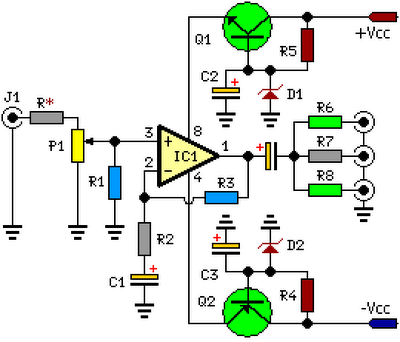
- Three Channel Audio Splitter Circuit Diagram & Build Guide
- Build a 500Hz-2Khz Notch Filter with 0.1uF & 1.5K Resistors
- Build Your 1700Hz Op-Amp Bandpass Filter Circuit
- Build Stunning 2nd Order Opamp Filters – Design Guide
- Craft a 300-3kHz Bandpass Filter Circuit Diagram
- Separate Stereo Bass: A Circuit for Clarity
- Variable High-Pass Filter: 20Hz to 200Hz Design
Three Channel Audio Splitter Circuit Diagram & Build Guide
Description
This circuit is designed for amplifying and distributing audio signals effectively. The audio input signal is applied to J1, subsequently passing through P1, where it undergoes buffering and amplification thanks to IC1, which is specifically configured for signal redistribution. It features three outputs capable of driving three audio lines, each with a 300-ohm impedance.
Circuit Diagram:
Parts:
- J1 = RCA Audio input female socket.
- P1 = 100K-Potentiometre
- R* = 10K-100K
- R1 = 560K
- R2 = 1K
- R3 = 2.2K
- R4 = 2.7K
- R5 = 2.7K
- R6 = 330R
- R7 = 330R
- R8 = 330R
- C1 = 100uF-25V
- C2 = 100uF-25V
- C3 = 100uF-25V
- D1 = BZX79C18
- D2 = BZX79C18
- Q1 = BC337
- Q2 = BC327
- IC1 = NE5532-34
Notes:
- J1 will be RCA Audio input female socket.
- R* is on your choice it can be choose between 10K to 100K resistor.
- Output capacitor’s value is between 100uf to 470uf and power handling is 25V to 50V.
- You can power up this circuit via +12V/-12V regulated supply but you have to remove following parts Q1-Q2-C2-C3-D1-D2.
- Maximum power ratings +35V/-35V
IC1 - NE5532-34
The NE5532-34 is a versatile operational amplifier (op-amp) widely employed in audio circuits. This particular variant is a three-terminal JFET op-amp, providing high input impedance, low noise, and excellent linearity. It’s commonly utilized for amplification, buffering, and signal conditioning in various audio applications. It operates from a single supply and is favored for its performance characteristics and readily available resources. Its key features include a wide bandwidth and good signal-to-noise ratio, making it suitable for demanding audio applications. The device's JFET input configuration offers superior input impedance, minimizing loading effects on the signal source.
