- Build Your "Who's First" Game Indicator Circuit!
- Build Your Own Electronic Dice: A 9V Circuit Design
- Build Your Digital Roulette Circuit Diagram
- Build Your Own 4017B Electronic Dice Circuit Diagram
- Build a Brilliant 30-Socket Circuit Game Schematic
- Build Your Magnetic Gun: A 18V Circuit Design
- Build Your 4 Input Quiz Circuit Diagram
- Build a Magnetic Circuit: The 1-2-3 Wand Trick
Build Your 4 Input Quiz Circuit Diagram
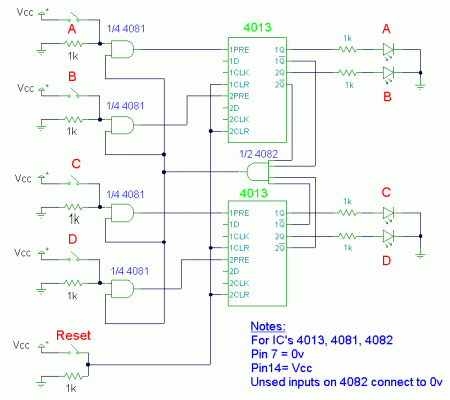
Several requests have been received for a test circuit, and consequently, a four-input design is presented here, easily adaptable for modification. It might be worthwhile to develop application notes in the style of a game show presenter...
Circuit Diagram
Notes:
- This design incorporates four integrated circuits and features four input circuits alongside four independent outputs, alongside a single master reset switch. The outputs, in this instance, are LED's, yet they may be modified to control lamps or buzzers. Only one output LED can illuminate simultaneously. The initial input press by individuals utilizing switches A, B, C, or D will activate the corresponding output LED, disabling the other input switches.
- The circuit utilizes exclusively CMOS integrated circuits, as indicated on the diagram. The supply voltage can range from 3 to 15 volts. Alternatively, it may be constructed employing equivalent TTL integrated circuits and powered with a 5-volt supply. A central element within this circuit is a bistable latch, and it’s based on the dual 4013 D-type flip-flop.
Integrated Circuit Description
The dual 4013 is a versatile integrated circuit that serves as a fundamental building block in digital logic circuits. It is a D-type flip-flop, meaning it can store one bit of data – either a logic 0 or a logic 1. The 4013 consists of two independent flip-flops, allowing for the creation of more complex logic functions. These flip-flops are controlled by clock signals, enabling them to transition between their high and low states. The dual 4013 is commonly used in applications such as counters, shift registers, and memory elements. Its compact size and low power consumption make it a popular choice for embedded systems and other resource-constrained designs. It can be utilized in a variety of digital circuits. Its flexibility allows for a multitude of applications. The flip-flop is essential in digital circuits. It’s commonly found in electronic devices. Its key characteristic is storing data.
Circuit Operation:
Activating the reset switch will restore the entire circuit to its initial state, clearing all flip-flops and extinguishing any illuminated LED's. Under this condition, the Q outputs will be low (logic 0), and the NOT Q outputs will be high (logic 1). All four NOT Q outputs are connected to an input of a 4-input AND gate (4082), whose output will also be high. The output of the 4082 is wired to an input of each 2-input AND gate (4081). The input switches A, B, C, and D are non-latching push buttons. The first individual to depress their corresponding switch will cause the linked AND gate (4081) to become high, triggering the preset input of the dual 4013 D-type flip-flop. This, in turn, will latch and illuminate the appropriate LED. Furthermore, the triggered flip-flop will have its NOT Q output set to low, which changes the 4082 output to low, thereby preventing further activation of the other flip-flops. De-bouncing of switch contacts is not necessary, as the initial press will latch one of the bistable states. Activating the reset switch will restore the circuit to its previous state. It is recommended to use robust push button switches, as they may be subjected to stress during operation.
circuit from http://www.zen22142.zen.co.uk/
