- Protect Your Line: Building a Lightning Surge Shield
- Build a Telephone Ringer: Circuit & Control
- Cellular Phone Call Detector: Build Your Own Schematic
- Telephone Amplifier Circuit Diagram – Boost Your Voice!
- Build a Cell Phone Call Detector with Flashing LED
- Ringing Phone Light Flasher Circuit Diagram Build Guide
- Soft Musical Ringer Circuit Diagram: Build Your Own!
- Build a 48V Hold Music Circuit Diagram
Cellular Phone Call Detector: Build Your Own Schematic
Description
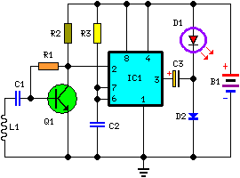
This circuit was created to identify when a telephone call is arriving in a cellular device (even if the caller’s tone setting within the device is deactivated) through the use of a glowing LED. The apparatus needs to be positioned approximately several centimeters away from the cellular phone, so its detection coil L1 can perceive the field produced by the phone’s receiver during an incoming call.
Circuit Diagram:
Components:
- R1 = 100K
- R2 = 3.9K
- R3 = 1M
- C1 = 100nF - 63V
- C2 = 100nF - 63V
- C3 = 220µF - 25V
- D1 = Red LED, 10mm diameter - Ultra-bright (refer to the Notes)
- D2 = 1N5819 - 40V, 1A Schottky Barrier Diode (refer to the Notes)
- Q1 = BC547 - 45V, 100mA NPN Transistor
- L1 = Sensor coil (refer to the Notes)
- B1 = 1.5V Battery (AA or AAA cell, etc.)
- IC1 = 7555 or TS555CN CMOS Timer IC
Circuit Operation:
The signal sensed by the detection coil is boosted by transistor Q1 and is fed into the control input pin of IC1. The IC’s output voltage is doubled utilizing C2 & D2 to power the high-efficiency, ultra-bright LED at an appropriate peak voltage.
Notes:
- The current consumption in the standby mode is less than 200µA; therefore, a power on/off switch is not required.
- The sensitivity of this circuit depends on the characteristics of the sensor coil.
- L1 can be fabricated by winding 130 to 150 turns of 0.2 mm enameled wire around a 5 cm diameter former (e.g., a can). Remove the coil from the former and insulate it with tape to create a separate coil.
- A commercially available 10mH miniature inductor, commonly found packaged in a small rectangular plastic enclosure, can also be used successfully, though with reduced sensitivity.
- IC1 must be a CMOS type device; only these types are safe for operation at 1.5V or lower supply voltages.
- Any Schottky barrier type diode can be substituted for the 1N5819; the BAT46 is a particularly suitable selection.
Integrated Circuit Description
The 7555, often referred to as TS555CN, is a versatile CMOS timer IC renowned for its stable operation and ease of use. This integrated circuit functions as a monostable multivibrator, generating a timed pulse when triggered. The IC’s internal circuitry incorporates a capacitor and a transistor to create a reliable timing circuit. Its CMOS technology ensures low power consumption and predictable behavior, making it suitable for a wide range of applications. The IC operates efficiently at low supply voltages, typically 1.5V or less, and exhibits a robust output signal. Its operation is precisely controlled by adjusting external components, enabling the user to fine-tune the timing interval. Furthermore, the IC’s CMOS construction enhances its resistance to noise and temperature fluctuations, ensuring a stable and reliable output over varying conditions. It's commonly utilized in pulse generation, timing circuits, and oscillator designs. This particular IC has a high degree of integration, incorporating essential components within a single package, simplifying circuit design and reducing component count. Its digital nature provides enhanced control and adaptability, furthering its versatility in electronic projects. The CMos construction of this IC enhances its reliability and performance due to its resistance to electrical noise and temperature variations. This contributes to the long-term stability and predictability of the circuit in which it is used.
