- Simple 4 Transistor Hearing Aid Circuit Diagram
- Amplified Ear: Build a Sensitive Sound Amplifier
- Build Your Own 3V Hearing Aid Circuit Diagram
- Studio Stereo Headphone Amplifier Circuit Diagram
- Stereo Headphone Amplifier: Build Your 90mR Circuit
- 427mW Class-A Headphone Amp
- Portable Headphone Amp: Circuit & 3.7V Upgrade
- 100mW Headphone Amplifier Schematic Build Guide
- LME49830 High Power Amplifier Circuit Diagram
- TDA7052 Speech Amplifier Circuit Diagram & Build Guide
- DC-Coupled Audio Amplifier Design: A Practical Guide
- Build a Low-Power IR Audio Amplifier Circuit Diagram
- 8 Watt Audio Amplifier Schematic: Build Your Powerful Project
- 7 Watt TDA2003 Audio Amplifier Circuit Design
- High-Power 60W Audio Amplifier Schematic Design
DC-Coupled Audio Amplifier Design: A Practical Guide
Description
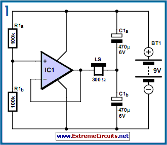
Designs for audio amplifiers utilizing DC coupling to the load are rarely seen today, despite presenting distinct benefits. A key advantage is the absence of the complexity associated with a secondary (balanced) power supply; another is a favorable frequency and phase response. Furthermore, specialized electrolytic capacitors for voltage stabilization are unnecessary, and the initial ‘thump’ experienced upon powering up is significantly diminished. To revive this circuit type from obsolescence, the author has developed a headphone amplifier, as depicted in Figure 1.
Integrated Circuit Details
IC1, a complex semiconductor device, plays a pivotal role in this amplifier design. This integrated circuit incorporates numerous transistors and diodes within a single package, enabling high-gain amplification with low distortion. It’s a common component in audio circuits due to its ability to boost weak audio signals to a level suitable for driving loudspeakers. The specific model used in this circuit offers a high-performance solution for audio amplification, providing both current gain and voltage gain.
Circuit Diagram:
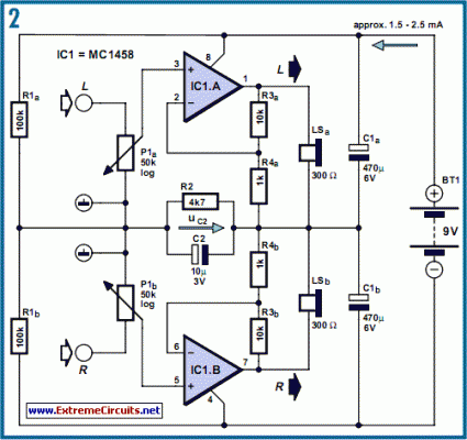
The circuit comprises a voltage divider, a voltage follower, and the loudspeaker connected to the headphones, whose other side is linked to the junction of two electrolytic capacitors, creating a virtual ground. The voltage at this point is, predictably, half of the power supply voltage. The task now is to effectively introduce the audio signal intended for amplification. Figure 2 illustrates a practical embodiment of this concept, forming a stereo headphone amplifier. The amplifier itself consists of IC1 and P1, along with R3 and R4, achieving a gain of 11.
Circuit Diagram:
This portion of the circuit necessitates no further elaboration, and the same holds true for the voltage divider described previously, constructed using R1a and R1b. The signal is coupled in through the potentiometers. C2 and R2 serve a specialized function: C2 connects the bottom end of the potentiometers (ground for the input signal) to the virtual ground. However, this capacitor establishes a feedback path, which could potentially induce oscillation within the amplifier under certain conditions. R2 effectively dampens this tendency to oscillate.
It's feasible to calculate suitable values for these components, but it’s generally preferable to determine them experimentally. C2 must be large enough to mitigate the impact of stray electric fields, preventing unacceptable hum at the output. R2 should be adequately sized to ensure the amplifier’s virtual earth stabilizes rapidly after switch-on. The electrolytic capacitor’s polarity is irrelevant as no significant voltage develops across the network. To assess the circuit’s behavior, it is possible to attempt operation with the C2/R2 network shorted and observe the outcome using an oscilloscope. The stabilization time of the voltage at the virtual earth point is dependent on the degree of asymmetry present within the circuit.
Warning: Always exercise caution when working with electrical circuits. Incorrect wiring or component selection can lead to electrical shock, fire, or damage to equipment. Ensure the power supply is disconnected before making any modifications to the circuit. Consult a qualified electrician if you are unsure about any aspect of the circuit design or construction. The author and source of this circuit diagram are acknowledged. Security is paramount; unauthorized modifications or distribution are strictly prohibited.
circuit from http://www.extremecircuits.net/2010/05/dc-coupled-audio-amplifier.html

