- Relay Control with Logic Levels: Resistor Guide
- Monostable Flip Flop Circuit: Build Your Timing Delay
- Bistable Flip Flop Circuit: Build Your Stable Electronic Switch
- Set/Reset Flip Flop: Build Your 1-Bit Memory Circuit
- Build Your Own 4017 LED Traffic Light Circuit Diagram
- Build Your 7490 Frequency Divider: A Powerful 2-10 Circuit
- Frequency Doubler: Build Your 4011 Circuit Diagram
- Build a 4069 Frequency Doubler Circuit Diagram
- Build a 50Hz to 25Hz Frequency Divider Circuit
- Build Your Classic MM5314N Digital Clock Circuit
- Step Km Counter Circuit Design
- Build Your 7 Segment LED Counter with a 74LS90
- Build Your Pocket Distance Counter!
Build a 4069 Frequency Doubler Circuit Diagram
Description
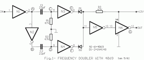
This frequency multiplier utilizing a single 4069 hex inverter IC, a frequency multiplier can be built to provide an output waveform whose frequency is doubled compared to a squarewave input signal. The signal is applied to the input of N1. It should be a squarewave with a duty-cycle of approximately 50% at a level compatible with CMOS logic (3-15V peak to peak depending on supply voltage). The input signal is buffered and inverted by N1, and then inverted again by N2, so the outputs A and B of N1 and N2 are squarewave signals 180° out of phase. The output of N1 is differentiated by C1 and R1, and the output of N2 is differentiated by C2 and R2, yielding two spike waveforms of C and D, 180° out of phase. The signals are buffered, inverted, and shaped by N3 and N4. These are then combined in a NOR gate consisting of D1, D2, R3 and N5, and finally inverted by N6 to generate the output frequency, which is twice that of the initial input signal. The circuit is designed for operation across a broad range of frequencies. With the specified component values, the pulse width at the E and F points is approximately 500ns, resulting in a 50% duty cycle of the output when the input frequency is 1MHz. When the input frequency is 500kHz, the output duty cycle is 50%.
Circuit diagram
circuit from http://users.otenet.gr/~athsam/frequency_doubler_with_4069.htm
