- Build a 4-Stage Stabilised Power Supply with Short Circuit Protection
- Build Your Own 3-30V Adjustable DC Power Supply
- Build Your Own 9V 2A DC Power Supply Circuit
- Build Your Own: 1.3-22V Adjustable Power Supply Circuit
- Adjustable Current Limit: Dual Power Supply Design
- Build Your High-Performance 170V Hybrid Amplifier Power Supply
- Build Your 15V Regulated Power Supply Circuit – Simple & Powerful
- Transformerless 5V Power Supply Design Guide
- Build Your Own 24V 2A Variable DC Power Supply
- High Voltage Regulator: Design and Short Circuit Protection
- Boost Regulator Current: Design Your 1500mA Circuit
- Extend Smoke Alarm Battery Life with 12V Power
- 2 Watt Switching Power Supply: Build Your Own Circuit
- Variable Voltage & Current Power Supply: Build Your 0-3 Amp Circuit
- Build Your 24 Volt 3 Amp Power Supply Circuit
Build Your Own Virtual Ground: 2SC1384 & 2SA684 Circuit
Description
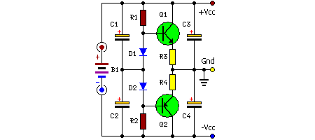
A straightforward virtual earth circuit utilizing individual components is presented here. This uncomplicated design originates from the expertise of miniaturization specialist Sijosae. The objective is to construct a signal amplifier utilizing readily available discrete elements. The transistors can be chosen from various complementary pairs of small-signal transistors. Appropriate replacements include the PN2222A and PN2907A. The diodes are typical small-signal types. The 1N914 represents a viable alternative. This configuration demonstrates superior functionality compared to a basic resistive divider virtual earth, and the cost of the components is less than that of any other circuit detailed within this collection. Nevertheless, it is considered the least precise buffered virtual earth circuit.
Circuit diagram:
Parts:
- R1,R2 = 4.7K
- R3,R4 = 4.7R
- C1,C2 = 470uF-25V
- C3,C4 = 47uF-25V
- D1,D2 = 1N4148
- Q1 = 2SC1384
- Q2 = 2SA684
- B1 = Battery
More about components
Integrated circuits, or ICs, play a crucial role in modern electronic design, offering a consolidated approach to circuit functionality. These components contain a large number of interconnected transistors, resistors, capacitors, and other components fabricated on a single semiconductor material, typically silicon. The PN2222A and PN2907A transistors, frequently employed in this circuit, are examples of these ICs. These integrated circuits are manufactured using complex fabrication processes and represent a significant advancement over discrete transistors. They provide increased reliability, reduced size, and improved performance characteristics. These ICs are typically packaged in small ceramic or plastic packages, offering a convenient way to integrate multiple functions into a single component. The 2SC1384 and 2SA684 are N-channel and P-channel MOSFETs, respectively, commonly used as switches or amplifiers within the circuit. Their integration provides a compact and efficient solution, simplifying the overall design and reducing component count. These ICs are selected for their low on-resistance, fast switching speeds, and low gate drive requirements, ensuring optimal performance in the circuit application. Their selection is critical for achieving the desired signal amplification and buffering capabilities.
Warnings
Please be aware that modifications to any of the circuits presented here could potentially damage the components or cause malfunctions. Always exercise caution when experimenting with electrical circuits. It is the responsibility of the user to ensure they understand the risks involved and to take appropriate safety measures. This collection is provided as a resource for educational and experimental purposes only. The authors are not liable for any damages or injuries resulting from the use of these circuits. Always consult with a qualified electronics professional if you are unsure about any aspect of circuit design or construction. This circuit uses a battery, and improper handling of batteries can lead to hazardous situations. Follow all safety precautions associated with battery use. This collection is provided without warranty of any kind, express or implied.
Author and Source
Circuit diagram provided by Sijosae. Source: [https:/www.youtube.com/watch?v=cM8k7l2D8Xw](https://www.youtube.com/watch?v=cM8k7l2D8Xw)
