similar circuits
- 9V FM Transmitter Circuit: Build Your 100m Range
- Opamp VHF FM Transmitter Design (88-108 MHz)
- Build Your Own 50m Stereo Wireless Audio Link Circuit
- FM 45W Valve Transmitter Circuit Diagram – Build Your Own!
- Build Your Own 85-108 MHz Radio Transmitter!
- 3W FM Transmitter Schematic Blueprint
- Build Your Own 2 Transistor FM Voice Transmitter Circuit
- Build Your 88-108MHz 4W FM Transmitter Circuit
- FM Transmitter Bug: 4 Turns, 1.5 Turns – Build Your Circuit
- Build Your Own 98 MHz FM Beacon Transmitter
3W FM Transmitter Schematic Blueprint
Description
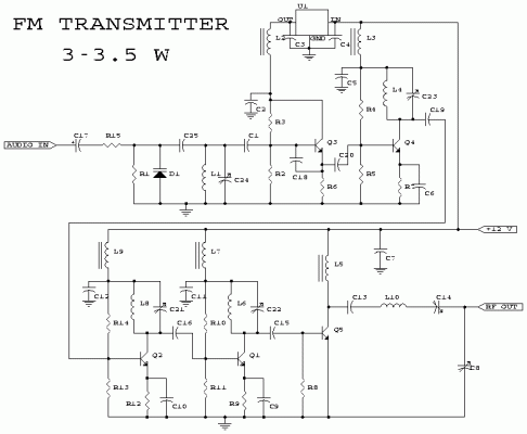
This schematic illustrates an FM transmitter, capable of generating an output power ranging from 3 to 3.5 Watts, operating within the frequency band of 90 to 110 MHz. While the circuit's stability isn't exceptionally high, the incorporation of a Phase-Locked Loop (PLL) can significantly improve its performance.
This circuit was constructed several years ago for a friend, who utilized it in conjunction with the BLY88 amplifier to achieve an output power of 20 Watts. Based on the initial schematic documentation, the circuit functioned reliably with a Standing Wave Ratio (SWR) of 1 : 1.05, a value considered normal within my environment, considering the antenna setup.
Circuit diagram
Parts:
- R1, R4, R14, R15: 10kΩ, 1/4W Resistor
- R2, R3: 22kΩ, 1/4W Resistor
- R5, R13: 3.9kΩ, 1/4W Resistor
- R6, R11: 680Ω, 1/4W Resistor
- R7: 150Ω, 1/4W Resistor
- R8, R12: 100Ω, 1/4W Resistor
- R9: 68Ω, 1/4W Resistor
- R10: 6.8kΩ, 1/4W Resistor
- C1: 4.7pF Ceramic Disc Capacitor
- C2, C3, C4, C5, C7, C11, C12: 100nF Ceramic Disc Capacitor
- C6, C9, C10: 10nF Ceramic Disc Capacitor
- C8, C14: 60pF Trimmer Capacitor
- C13: 82pF Ceramic Disc Capacitor
- C15: 27pF Ceramic Disc Capacitor
- C16: 22pF Ceramic Disc Capacitor
- C17: 10uF, 25V Electrolytic Capacitor
- C18: 33pF Ceramic Disc Capacitor
- C19: 18pF Ceramic Disc Capacitor
- C20: 12pF Ceramic Disc Capacitor
- C21, C22, C23, C24: 40pF Trimmer Capacitor
- C25: 5pF Ceramic Disc Capacitor
- L1: 5 WDG, Diameter 6 mm, 1 mm CuAg, Air Gap 1 mm
- L2, L3, L5, L7, L9: 6-hole Ferroxcube Wide Band HF Choke (5 WDG)
- L4, L6, L8: 1.5 WDG, Diameter 6 mm, 1 mm CuAg, Air Gap 1 mm
- L10: 8 WDG, Diameter 5 mm, 1 mm CuAg, Air Gap 1 mm
- D1: BB405 or BB102 or equivalent (most varicaps with C = 2-20 pF [approximately] will suffice)
- Q1: 2N3866
- Q2, Q4: 2N2219A
- Q3: BF115
- Q5: 2N3553
- U1: 7810 Regulator
- MIC: Electret Microphone
- MISC: PC Board, Wire for Antenna, Heatsinks
Notes:
- Contact Rae XL Tkacik via email with any inquiries, feedback, or comments.
- This circuit has been tested on a standard RF-testing breadboard (with one side featuring copper connections). Establish connections between the two sides of the breadboard. Construct the transmitter within a shielded RF-proof casing, employ high-quality connectors and cables, and implement shielding measures between various stages. Be mindful of all relevant RF rules and regulations during the construction process.
- Q1 and Q5 require heat sinking. The case pin of Q4 must be connected to ground.
- C24 serves as a frequency adjustment component. The other trimmer capacitors should be adjusted to achieve maximum output power while minimizing the SWR and input current.
- Local regulations in certain states, provinces, or countries may prohibit the operation of this transmitter. Verify compliance with local authorities prior to operation.
author: Rae XL Tkacik, vocko@atlas.cz
circuit from http://www.aaroncake.net/circuits/index.asp
circuit from http://www.aaroncake.net/circuits/index.asp
