- 9V FM Transmitter Circuit: Build Your 100m Range
- Opamp VHF FM Transmitter Design (88-108 MHz)
- Build Your Own 50m Stereo Wireless Audio Link Circuit
- FM 45W Valve Transmitter Circuit Diagram – Build Your Own!
- Build Your Own 85-108 MHz Radio Transmitter!
- 3W FM Transmitter Schematic Blueprint
- Build Your Own 2 Transistor FM Voice Transmitter Circuit
- Build Your 88-108MHz 4W FM Transmitter Circuit
- FM Transmitter Bug: 4 Turns, 1.5 Turns – Build Your Circuit
- Build Your Own 98 MHz FM Beacon Transmitter
Build Your Own 85-108 MHz Radio Transmitter!
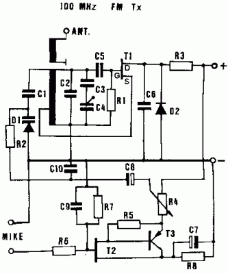
Circuit diagram
DESCRIPTION
This document details the construction of a small radio transmitter, featuring a Printed Circuit Board (PCB) measuring 1.75" x 2.5" (45mm x 68 mm) and offering a range of approximately 30 yards. The accompanying documentation specifies a frequency range of 100-108 MHz, though testing has revealed a more typical operational range between 85-100 MHz. The circuit is mono in design and accepts an audio input from sources like a microphone or similar. The input impedance is 1Mohm, with an input sensitivity of 5mV and a maximum input signal level of 10mV. The transmitted signal can be detected on an FM radio receiver. This circuit is suitable for short-range transmissions, such as those used in wireless microphone applications. The circuit originates from a ‘Kit’, available from Veleman electronics (USA distributor is Tapto Corp., PO Box 1339, CLAREMONT NH-03743-US. UK distributor is High-Q Electronics, 382 Edgware Road, London, W2 1EB). The kit number is K1771. This kit represents a very effective transmitter. I acquired the kit and assembled the circuit, which performed reliably. To create two transmitters, I developed a custom PCB and built the circuit, and my homemade version ultimately demonstrated superior performance compared to the original. Therefore, purchasing the kit is not essential, as the circuit is relatively straightforward and represents a well-regarded ‘home-made’ transmitter. CIRCUIT.GIF illustrates the circuit diagram. PCBPLAN.GIF visually depicts the PCB layout, showing the placement of components. PCBPLAN.GIF provides a precise layout, scanned directly from the instruction sheet. A reference corner is marked with an asterisk for ease of alignment. TRACKS.GIF displays the track layout on the side of the board intended for soldering. It’s important to note that this layout is not perfectly accurate, as a dedicated track plan was not initially created. To generate TRACKS.GIF, I utilized OHP film, tracing the tracks with an OHP pen, and subsequently scanned the result. The component leg holes are approximately indicated with white blobs.
CONSTRUCTION
Initially, scale PCBPLAN.GIF and TRACKS.GIF to match the desired overall dimensions of approximately 1.75" x 2.5". Subsequently, fabricate the PCB. As PCBPLAN.GIF indicates the accurate positioning of the holes, while TRACKS.GIF offers only approximate positions, utilize PCBPLAN when drilling holes in the PCB board. Then, trace the tracks, guided by TRACKS.GIF. It’s crucial to ensure correct reproduction of the 'printed coil' on the PCB – these lines are present for a specific reason!
Parts
- D1 Varicap diode (e.g., BB119)
- D2 1N4148
- R1 100K
- R2 220K
- R3 22R
- R4 1K trimmer
- R5 1K
- R6 56K
- R7 1M
- R8 1K2
- C1 5pF ceramic
- C2 6pF ceramic
- C3 15pF ceramic
- C4 trimmer cap
- C5 15pF ceramic
- C6 1nF ceramic
- C7 100uF electrolytic
- C8 4.7uF electrolytic
- C9 100pF ceramic
- T1 BF244A or BF245A FET
- T2 2N3819 FET
- T3 BC307/8/9 or BC557/8/9 PNP
Bear in mind that, in addition to the components, a jumper wire needs to be fitted (marked with a dashed line in PCBPLAN.GIF). The power supply should be a 9-14 V DC source, a single rectangular 9V battery being suitable. Connect this to the + and - points on the PCB. The sound input should be directed to the points marked “MIKE”. The antenna should be connected to the point marked “ANT”. The emitter's output impedance is 50 ohms. A custom antenna can be fashioned if desired; however, a length of approximately one foot of wire is generally sufficient.
Good luck with the transmitter. If you have any improvements to the circuit, I would be glad to hear from you. --Dan Evans.
circuit from http://sable.ox.ac.uk/~sjoh0014/web/dan.html
