- Simple 4 Transistor Hearing Aid Circuit Diagram
- Amplified Ear: Build a Sensitive Sound Amplifier
- Build Your Own 3V Hearing Aid Circuit Diagram
- Studio Stereo Headphone Amplifier Circuit Diagram
- Stereo Headphone Amplifier: Build Your 90mR Circuit
- 427mW Class-A Headphone Amp
- Portable Headphone Amp: Circuit & 3.7V Upgrade
- 100mW Headphone Amplifier Schematic Build Guide
- LME49830 High Power Amplifier Circuit Diagram
- TDA7052 Speech Amplifier Circuit Diagram & Build Guide
- DC-Coupled Audio Amplifier Design: A Practical Guide
- Build a Low-Power IR Audio Amplifier Circuit Diagram
- 8 Watt Audio Amplifier Schematic: Build Your Powerful Project
- 7 Watt TDA2003 Audio Amplifier Circuit Design
- High-Power 60W Audio Amplifier Schematic Design
Build Your Own: Mini-Box 2W Amplifier Circuit Diagram
Designed for self-powered 8, 4 & 2 Ohm loudspeakers
Bass-boost switch
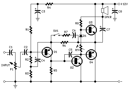
Circuit diagram:
Parts:
- P1 = 10K Log.Potentiometer
- R1,R2 = 33K 1/4W Resistors
- R3 = 33R 1/4W Resistor
- R4 = 15K 1/4W Resistor
- R5,R6 = 1K 1/4W Resistors
- R7 = 680R 1/4W Resistor
- R8 = 120R 1/2W Resistor
- R9 = 100R 1/2W Trimmer Cermet
- C1,C2 = 10uF 63V Electrolytic Capacitors
- C3 = 100uF 25V Electrolytic Capacitor
- C4,C7 = 470uF 25V Electrolytic Capacitors
- C5 = 47pF 63V Ceramic Capacitor
- C6 = 220nF 63V Polyester Capacitor
- C8 = 1000uF 25V Electrolytic Capacitor
- D1 = 1N4148 75V 150mA Diode
- Q1 = BC560C 45V 100mA PNP Low noise High gain Transistor
- Q2 = BC337 45V 800mA NPN Transistor
- Q3 = TIP31A 60V 4A NPN Transistor
- Q4 = TIP32A 60V 4A PNP Transistor
- SW1 SPST switch
- SPKR 3-5 Watt Loudspeaker, 8, 4 or 2 Ohm impedance
Device purpose:
This amplifier was developed to be self-contained within a small loudspeaker enclosure. It can be powered by Walkman, Mini-Disc, and CD players, as well as computers and similar devices equipped with line or headphone outputs. Notably, a stereo configuration will necessitate the construction of two separate enclosures. The circuit’s design deliberately avoids the utilization of integrated circuits to achieve optimal harmonic distortion characteristics and to ensure the availability of components. The amplifier(s) are conveniently supplied via a 12V wall plug-in transformer. Activating SW1 enables a bass-boost function, simultaneously requiring an increase in the volume control setting to compensate for power loss at higher frequencies. During operation, R9 should be carefully adjusted to produce minimal audible signal crossover distortion, consistent with a minimal measured quiescent current consumption; an appropriate compromise would be to set the quiescent current at approximately 10-15 mA. To measure this current, a DC current meter can be temporarily connected in series with the collector of Q3.
Technical data:
- Output power: 1.5 Watt RMS @ 8 Ohm, 2.5 Watt @ 4 Ohm, 3.5 Watt @ 2 Ohm (1KHz sinewave)
- Sensitivity: 100mV input for 1.5W output @ 8 Ohm
- Frequency response: 30Hz to 20KHz -1dB
- Total harmonic distortion @ 1KHz & 10KHz: Below 0.2% @ 8 Ohm 1W, below 0.3% @ 4 Ohm 2W, below 0.5% @ 2 Ohm 2W
Integrated Circuits:
BC560C
The BC560C is a general-purpose NPN transistor widely used in amateur radio and low-power electronic circuits. This transistor exhibits low noise and high gain characteristics, making it suitable for amplification applications. It operates with a collector-emitter voltage of 45V and a continuous collector current of 100mA.
BC337
The BC337 is a general-purpose NPN transistor frequently employed in low-power circuits and audio amplifiers. It provides good stability and reliability, making it a dependable choice for a range of applications. This transistor can deliver an 800mA continuous collector current at a collector-emitter voltage of 45V.
TIP31A
The TIP31A is a high-current NPN transistor designed for driving inductive loads such as motors and relays. It offers robust current handling capabilities and features a continuous collector current rating of 4A at a collector-emitter voltage of 60V. It’s commonly found in switching power supplies and motor control circuits.
TIP32A
The TIP32A is a high-current PNP transistor designed for driving inductive loads similar to the TIP31A but with a PNP configuration. It can deliver a continuous collector current of 4A at a collector-emitter voltage of 60V. This component is often utilized in switching power supplies and motor control circuits, offering a complementary option to the TIP31A.
