- Simple 4 Transistor Hearing Aid Circuit Diagram
- Amplified Ear: Build a Sensitive Sound Amplifier
- Build Your Own 3V Hearing Aid Circuit Diagram
- Studio Stereo Headphone Amplifier Circuit Diagram
- Stereo Headphone Amplifier: Build Your 90mR Circuit
- 427mW Class-A Headphone Amp
- Portable Headphone Amp: Circuit & 3.7V Upgrade
- 100mW Headphone Amplifier Schematic Build Guide
- LME49830 High Power Amplifier Circuit Diagram
- TDA7052 Speech Amplifier Circuit Diagram & Build Guide
- DC-Coupled Audio Amplifier Design: A Practical Guide
- Build a Low-Power IR Audio Amplifier Circuit Diagram
- 8 Watt Audio Amplifier Schematic: Build Your Powerful Project
- 7 Watt TDA2003 Audio Amplifier Circuit Design
- High-Power 60W Audio Amplifier Schematic Design
Build Your 8W TDA2005 Stereo Amplifier Circuit
Description
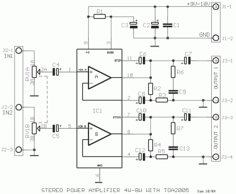
A class AB stereo audio power amplifier, designed by Quasar for high-fidelity applications, utilizing a TDA2005 module, is presented here. This circuit is characterized by its straightforward construction and minimal external component count. The integrated module incorporates output current and thermal protection mechanisms. The resultant sound quality is excellent. The required power supply voltage ranges from 9V to 18V DC, delivering a current of 1 to 2 Amps. Optimal power output is achieved with a power supply of at least 2A at 15V DC, alongside the use of 2 Ohm or 4 Ohm speakers in parallel configurations. Approximately 4W/ch. can be realized with a 15V DC, 1A supply and 4-ohm loads.
TDA2005
The TDA2005 is a dual integrated circuit, a power amplifier IC designed by Texas Instruments. It is a popular choice for audio amplifier applications due to its high efficiency and low distortion characteristics. It's a monolithic integrated circuit containing two independent Class AB audio power amplifiers. It is commonly used in portable audio devices, small hi-fi systems, and automotive audio applications. This particular IC is a highly reliable and cost-effective solution for amplifying audio signals.
C4-5 represent input coupling capacitors which effectively block DC voltages, similar to C9-13, which also function as output coupling capacitors. Furthermore, C8-12 act as DC blockers, preventing DC current from flowing through the feedback loop to the differential inputs. R2-3 and R4-5 are employed to adjust the level of feedback. C9/R6 and C13/R7 are strategically included to provide a high-frequency load, ensuring stability when the inductive reactance of the loudspeaker becomes excessive. C1-2 serves for power supply decoupling or filtering. The gain achieved is equal to 1+(R2/R3)=1+(R4/R5)=37, or 31dB, minus any input attenuation. Increasing the feedback resistors R3 and R5 may increase the gain. The operational limits for the power supply voltage is 18V. Before connecting to the circuit, it is imperative to verify the power supply voltage and its polarity.
Circuit diagram
Parts list
- R1=120Kohm 1/2W 5%
- R2-4=1.2Kohm 1/4W 5%
- R3-5=33 ohm 1/4W 5%
- R6-7=1 ohm 1/2W 5%
- RV1=2X10Kohm Log. Pot.
- C1-9-13=100nF 100V MKT
- C2=220uF 25V
- C3=10uF 25V
- C4-5=2.2uF 25V
- C6-10=100uF 25V
- C7-11=2200uF 16V
- C8-12=220uF 25V
- IC1=TDA2005
- J1=2 Pole Terminal Block
- J2-3=3 Pole Terminal Block
Specifications
- Power Supply 918V at 12 A
- Power output:
- >8 W RMS/ch. at 2ohm 16V DC supply.
- >6W RMS/ch.at 4ohm 16V DC supply
- >4W RMS/ch.at 4ohm 12V DC supply
- THD <0.1% @ 1W, 4ohm, 0.018% at 1W RMS @ 4 ohm and +15V supply
- Frequency response ~15 Hz to 50 kHz, 3 dB
- S/N ratio >80 dBA.
- Input level ~160 mV for full output
- Gain ~31 dB maximum.
