- Simple 4 Transistor Hearing Aid Circuit Diagram
- Amplified Ear: Build a Sensitive Sound Amplifier
- Build Your Own 3V Hearing Aid Circuit Diagram
- Studio Stereo Headphone Amplifier Circuit Diagram
- Stereo Headphone Amplifier: Build Your 90mR Circuit
- 427mW Class-A Headphone Amp
- Portable Headphone Amp: Circuit & 3.7V Upgrade
- 100mW Headphone Amplifier Schematic Build Guide
- LME49830 High Power Amplifier Circuit Diagram
- TDA7052 Speech Amplifier Circuit Diagram & Build Guide
- DC-Coupled Audio Amplifier Design: A Practical Guide
- Build a Low-Power IR Audio Amplifier Circuit Diagram
- 8 Watt Audio Amplifier Schematic: Build Your Powerful Project
- 7 Watt TDA2003 Audio Amplifier Circuit Design
- High-Power 60W Audio Amplifier Schematic Design
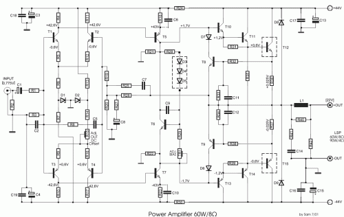
60W 8Ω Power Amplifier Circuit Diagram
Description
This circuit was developed and produced during the '80s and has functioned reliably since that time. It doesn’t present any particular constructional challenges, beyond the important considerations concerning the provided power supply – selecting an appropriate heatsink and ensuring a good match between the driver transistors. Diodes D3 through D9 should be mounted above the output transistors on the heatsink to facilitate thermal coupling. The trimmer resistor R15 is employed to precisely regulate the output voltage of the amplifier, which occasionally exhibits intermittent operation before stabilizing thermally. With the trimmer TR1, the amplifier’s bias current is set between 50 and 100 mA. This bias current can be measured by observing the voltage drop across the high-value resistors R36 and R37, yielding a current of approximately 75 mA under typical operating conditions. The voltage values indicated in the schematic are original values, however, they may possess a tolerance of approximately ±10%.
Circuit diagram
Parts list
- R1=1.8Kohm
- R2=220Kohm
- R3=27Kohm
- R4-10-11-17=3.3Kohm
- R5-9-12-16=100ohm
- R6=18Kohm
- R7-13=3.9Kohm
- R14=10Kohm
- R15=22Kohm Trimmer
- R18-23=330ohm
- R19-21-22=15Kohm
- R20=12Kohm
- R24-30=82ohm
- R25=8.2Kohm
- R26=27Kohm
- R27=820ohm
- R28=3.3Kohm
- R29=100ohm
- R31-39=180ohm
- R32-38=6.8Kohm
- R33-34=1.2Kohm
- R35=82ohm /1W
- R36-37=0.33ohm / 5W
- R40-41=10ohm / 2W
- R42=180ohm/5W
- TR1=4.7Kohm Trimmer
- D1-2=24V/1W Zener
- D3....9=1N4002
- T1-2=BC550C
- T3-4=BC560C
- T5-13=BD530
- T6-8=BC414C
- T9=BC416C
- T7-10=BD529
- T11=BD591
- T14=BD592
- T12=2N5630
- T15=2N6030
- C1=4.7uF/25V
- C2=470pF
- C3-4=100uF/63V
- C5=68pF
- C6-10=330pF
- C7=22pF
- C8=220uF/16V
- C9=100nF 100V
- C11-12=10pF
- C13-15=47uF/63V
- C16-17=100nF/100V
- C18-19=100nF/100V
