similar circuits
- Simple 4 Transistor Hearing Aid Circuit Diagram
- Amplified Ear: Build a Sensitive Sound Amplifier
- Build Your Own 3V Hearing Aid Circuit Diagram
- Studio Stereo Headphone Amplifier Circuit Diagram
- Stereo Headphone Amplifier: Build Your 90mR Circuit
- 427mW Class-A Headphone Amp
- Portable Headphone Amp: Circuit & 3.7V Upgrade
- 100mW Headphone Amplifier Schematic Build Guide
- LME49830 High Power Amplifier Circuit Diagram
- TDA7052 Speech Amplifier Circuit Diagram & Build Guide
- DC-Coupled Audio Amplifier Design: A Practical Guide
- Build a Low-Power IR Audio Amplifier Circuit Diagram
- 8 Watt Audio Amplifier Schematic: Build Your Powerful Project
- 7 Watt TDA2003 Audio Amplifier Circuit Design
- High-Power 60W Audio Amplifier Schematic Design
Build Your 18 Watt Audio Amplifier Circuit Today!
Circuit Diagram:
Amplifier components:
- P1 = 22K
- R1 = 1K
- R2 = 4K7
- R3 = 100R
- R4 = 4K7
- R5 = 82K
- R6 = 10R-1/2W
- R7 = 22R
- R8 = 1K-1/2W (optional)
- C1 = 470nF-63V
- C2 = 100µF-3V Tantalum bead Capacitors
- C3 = 470µF-25V
- C4 = 470µF-25V
- C5 = 100µF-3V Tantalum bead Capacitors
- C6 = 100nF-63V
- D1 = 1N4148
- IC1 = TLE2141C – This integrated circuit is a common amplifying device frequently utilized in radio frequency applications, offering low noise and high stability.
- Q1 = BC182 – This Bipolar Junction Transistor (BJT) is a general-purpose transistor, suitable for a variety of signal amplification and switching circuits.
- Q2 = BC212 50V 100mA PNP Transistor – A PNP transistor, providing high input impedance and suitable for switching applications.
- Q3 = TIP42A – A power transistor designed for high current applications, often utilized in audio amplifiers and switching circuits.
- Q4 = TIP41A – Another power transistor, commonly found in audio amplifier designs.
- J1 = RCA audio input socket
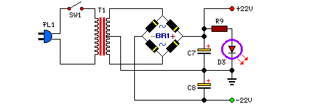
Power supply parts:
- R9 = 2K2
- C7 = 4700µF 25V
- C8 = 4700µF 25V
- D2 = 100V 4A Diode bridge – A high-current rectifier diode, capable of handling significant power dissipation.
- D3 = 5mm. Red LED – A standard red LED used for visual indication.
- T1 = 30VCT, 50VA Mains transformer – A mains transformer providing isolation and voltage transformation.
- PL1 = Male Mains plug
- SW1 = SPST Mains switch
Notes:
- This circuit can be directly connected to CD players, tuners, and tape recorders.
- It is imperative not to exceed 23 + 23V supply.
- Heat dissipation considerations are important; Q3 and Q4 must be mounted on suitable heatsinks.
- Thermal contact between D1 and Q1 is required for optimal performance.
- The quiescent current, when measured with an Avo-meter in series with Q3 Emitter, isn’t a critical parameter.
- The quiescent current can be adjusted by modifying R3 to achieve a reading between 20 to 30 mA when no input signal is present.
- To facilitate quiescent current adjustment, R8 (optional) may be incorporated.
- Correct grounding is absolutely vital to eliminate hum and ground loops. Connections should include the ground sides of J1, P1, C2, C3 & C4. Additionally, C6 must be connected to the output ground.
- Subsequently, the input and output grounds must be independently connected to the power supply ground.
