- Simple 4 Transistor Hearing Aid Circuit Diagram
- Amplified Ear: Build a Sensitive Sound Amplifier
- Build Your Own 3V Hearing Aid Circuit Diagram
- Studio Stereo Headphone Amplifier Circuit Diagram
- Stereo Headphone Amplifier: Build Your 90mR Circuit
- 427mW Class-A Headphone Amp
- Portable Headphone Amp: Circuit & 3.7V Upgrade
- 100mW Headphone Amplifier Schematic Build Guide
- LME49830 High Power Amplifier Circuit Diagram
- TDA7052 Speech Amplifier Circuit Diagram & Build Guide
- DC-Coupled Audio Amplifier Design: A Practical Guide
- Build a Low-Power IR Audio Amplifier Circuit Diagram
- 8 Watt Audio Amplifier Schematic: Build Your Powerful Project
- 7 Watt TDA2003 Audio Amplifier Circuit Design
- High-Power 60W Audio Amplifier Schematic Design
45 Watt Class-B Audio Amplifier Circuit Design
Description
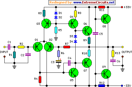
Discrete-component op-amps are employed in this design to drive a complementary Bipolar Junction Transistor (BJT) output stage, resulting in Class B operation. This configuration minimizes quiescent current when delivering low output currents, as the op-amp effectively shuts off the transistors. At higher output currents, the power transistors conduct, and the op-amp contributes only approximately 0.7/R11 to the overall output current. The op-amp’s quiescent current biases the external transistors, thereby significantly reducing the crossover frequency.
The concept originated from a letter published in Wireless World, December 1982, page 65, authored by N. M. Allinson, formerly at the University of Keele, Staffordshire. The letter proposed using op-amp ICs as drivers, but considering the required supply voltages (up to +/- 35V) for an amplifier generating roughly 50W, a discrete-component op-amp approach was deemed suitable and ultimately proved successful.
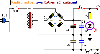
The discrete-component op-amp is based on a Douglas Self design. However, his original circuit featured a Class A output stage. To achieve the desired Class B operation, the circuit was subsequently modified accordingly. The amplifier is powered by a mains transformer supplying a secondary winding rated at a common value of 25 + 25V (or 24 + 24V) and 120VA power. This allows for driving two amplifiers at 45W and 69W output power into 8 and 4 Ohms respectively, exhibiting very low distortion (less than 0.01% @ 1kHz and 20W into 8 Ohms).
This simple, straightforward, and rugged circuit, designed for any high-quality audio application and, above all, to complement the recently initiated series of articles forming the Modular Preamplifier Control Center, is also ideally suited for constructing a good Guitar or Bass amplifier. Enjoy!
Integrated circuits, specifically op-amps, play a critical role in this amplifier’s functionality. Op-amps are used as drivers for the BJT output stage, ensuring a Class B operation. This configuration minimizes quiescent current when delivering low output currents, as the op-amp effectively shuts off the transistors. At higher output currents, the power transistors conduct, and the contribution of the op-amp is limited to approximately 0.7/R11 to the overall output current. The op-amp’s quiescent current biases the external transistors, thereby significantly reducing the crossover frequency. The precise control afforded by the op-amp is crucial for achieving the desired amplifier characteristics.
Circuit diagram:
Parts:
- R1______________18K - 1/4W Resistor
- R2_______________3.9K - 1/4W Resistor
- R3,R6____________1K - 1/4W Resistors
- R4_______________2.2K - 1/4W Resistor
- R5______________15K - 1/4W Resistor
- R7______________22K - 1/4W Resistor
- R8_____________330R - 1/4W Resistor
- R9,R10__________10R - 1/4W Resistors
- R11,R12_________47R - 1/4W Resistors
- R13_____________10R - 1W Resistor
- C1_______________1µF - 63V Polyester Capacitor
- C2_____________470pF - 63V Polystyrene or Ceramic Capacitor
- C3______________47µF - 25V Electrolytic Capacitor
- C4______________15pF - 63V Polystyrene or Ceramic Capacitor
- C6_____________220nF - 100V Polyester Capacitor
- C7_____________100nF - 63V Polyester Capacitor
Power supply :
Parts:
- R1_______________3.3K - 1/2W Resistor
- C1,C2_________4700µF - 50V Electrolytic Capacitors
- C3,C4__________100nF - 63V Polyester Capacitors
- D1_____________200V 8A Diode bridge
- D2_____________5mm. Red LED
- F1,F2__________4A Fuses with sockets
- T1_____________230V or 115V Primary, 25+25V Secondary 120VA Mains transformer
- PL1____________Male Mains plug
- SW1____________SPST Mains switch
Parts:
- Q1,Q2________BC560C - 45V 100mA Low noise High gain PNP Transistors
- Q3,Q4________BC556 - 65V 100mA PNP Transistors
- Q5___________BC546 - 65V 100mA NPN Transistor
- Q6___________BD139 - 80V 1.5A NPN Transistor
- Q7___________BD140 - 80V 1.5A PNP Transistor
- Q8__________2N3055 - 60V 15A NPN Transistor
- Q9__________MJ2955 - 60V 15A PNP Transistor
Comments:
The main design targets for this amplifier were as follows:
- Output power in the 40 - 70W range
- Simple circuitry
- Easy to locate, low cost components
- Rugged performance
- No setup
Notes:
- 2N3055 and MJ2955 transistors were listed for Q8 and Q9 as the preferred types, but many different output transistors can be used satisfactorily: TIP3055/TIP2955, TIP35/TIP36, MJ802/MJ4502 amongst others.
- Discrete op-amp output transistors Q6 and Q7 do not require any heatsink as their cases remain at ambient temperature. Power transistors Q8 and Q9 should be mounted on a black, finned heatsink as usual.

