- Long Delay Timer Circuit Diagram
- Jogging Timer Circuit Diagram
- Amplifier Timer Circuit Schematic
- A Very Useful Timed Beeper Circuit Schematic
- A Bedside Lamp Timer Circuit Schematic
- Safety Guard
- Midnight Security Light Circuit Schematic
- Power-Off Time Delay Relay
- Power-On Time Delay Relay
- Generating a Delayed Pulse Using The 555 Timer
- 555 timer Mono stable (one shot) circuit
- Generating Long Time Delays
- Low Voltage, High Current Time Delay Circuit
- 9 Second Digital Readout Countdown Timer
- 9 Second LED Timer and Relay Circuit
Generating a Delayed Pulse Using The 555 Timer
Description
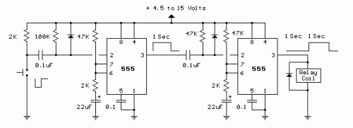
The circuit below illustrates generating a single positive pulse which is delayed relative to the trigger input time. The circuit is similar to the one above but employs two stages so that both the pulse width and delay can be controlled. When the button is depressed, the output of the first stage will move up and remain near the supply voltage until the delay time has elapsed, which in this case is about 1 second. The second 555 stage will not respond to the rising voltage since it requires a negative, falling voltage at pin 2, and so the second stage output remains low and the relay remains de-energized. At the end of the delay time, the output of the first stage returns to a low level, and the falling voltage causes the second stage to begin it's output cycle which is also about 1 second as shown. This same circuit can be built using the dual 555 timer which is a 556, however the pin numbers will be different.
