- Long Delay Timer Circuit Diagram
- Jogging Timer Circuit Diagram
- Amplifier Timer Circuit Schematic
- A Very Useful Timed Beeper Circuit Schematic
- A Bedside Lamp Timer Circuit Schematic
- Safety Guard
- Midnight Security Light Circuit Schematic
- Power-Off Time Delay Relay
- Power-On Time Delay Relay
- Generating a Delayed Pulse Using The 555 Timer
- 555 timer Mono stable (one shot) circuit
- Generating Long Time Delays
- Low Voltage, High Current Time Delay Circuit
- 9 Second Digital Readout Countdown Timer
- 9 Second LED Timer and Relay Circuit
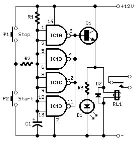
Long Delay Timer Circuit Diagram
Suitable for battery-operated devices, Fixed 35 minutes delay
This timer was designed mainly to switch off a portable radio after some time: in this way, one can fall asleep on the sand or on a hammock, resting assured that the receiver will switch off automatically after some time, saving battery costs.
Circuit operation:
R1 and C1 provide a very long time constant. When P2 is momentarily closed, C1 discharges and the near zero voltage at its positive lead is applied to the high impedance inputs of the four gates of IC1 wired in parallel. The four paralleled gate outputs of the IC go therefore to the high state and the battery voltage is available at Q1 Emitter.
When P2 is released, C1 starts charging slowly through R1 and when the voltage at its positive lead has reached about half the battery voltage, the IC gate outputs fall to zero, stopping Q1.
This transistor can directly drive a portable radio receiver or different devices drawing a current up to about 250mA. Connecting a Relay across the Emitter of Q1 and negative ground, devices requiring much higher voltage and current operation can be driven through its contacts.
Pushing on P2 for 1 to 5 seconds, the circuit starts and then will switch off after about 35 minutes. This time delay can be varied by changing R1 and/or C1 values. P1 will stop the timer if required.
LED D1 is optional and can be useful to signal relay operation when the load is placed far from the timer.
Circuit diagram:
Parts:
- R1______________10M 1/4W Resistor
- R2_______________4K7 1/4W Resistor
- R3_______________1K 1/4W Resistor (Optional, see Text)
- C1_____________220µF 25V Electrolytic capacitor
- D1______________LED any type and color (Optional, see Text)
- D2___________1N4148 75V 150mA Diode (Optional, see Text)
- IC1____________4011 Quad 2 Input NAND Gate CMos IC (See Notes)
- Q1____________BC337 45V 800mA NPN Transistor
- P1,P2__________SPST Pushbuttons
- RL1___________Relay with SPDT 2A @ 230V switch (Optional, see Text)
- Coil Voltage 12V - Coil resistance 200-300 Ohm
Notes:
- A 4011 Quad 2 Input NAND Gate was used for IC1, but many other CMos gates or inverter arrays can be used in its place, e.g. 4001, 4002, 4025, 4012, 4023, 4049, 4069. With these devices, all inputs must be tied together and also all outputs, as shown in the Circuit diagram.
- The operating voltage of this circuit should lie in the 6 - 12V range.
circuit from www.RedCircuits.com
