- Build Your 15-Second Courtesy Light Circuit Today
- Brightness Controller: Build a 1.5V LED/Lamp Circuit
- 12V DC Dimmer Circuit: Build Your Own Mood Lighting
- TRIAC Light Dimmer Circuit: Build Your 350W Dimmer
- Dome Lamp Dimmer Circuit: Build Your 700Hz Dimming System
- Build Your Automotive Lamp Dimmer: Circuit Diagram & Control
- Delayed Mains Lamp Circuit: Build Your 15-Second Timer
- 12 Volt Lamp Dimmer Circuit Diagram: Control Brightness with 555
- Sunrise Lamp Circuit: Build a 20-Minute Illumination Project
- 1.5 Hour Lamp Fader Sunset Lamp Circuit Diagram
- Build a 120V Lamp Dimmer: Full Wave Circuit Explained
- Build Your Inspiring 12 Volt Lamp Fader Circuit
- Illuminating Red Eyes
Delayed Mains Lamp Circuit: Build Your 15-Second Timer
Warning! The circuit is connected to 220Vac mains, then some parts in the circuit board are subjected to lethal potential!. Avoid touching the circuit when plugged and enclose it in a plastic box.
A suitable design for bedside lamps can be achieved through this circuit.
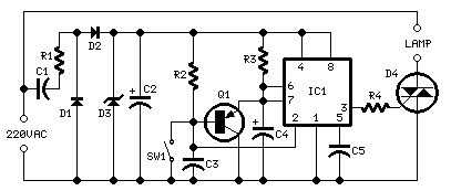
Circuit diagram
Parts:
- R1 470R 1/2W Resistor
- R2 100K 1/4W Resistor
- R3 1M5 1/4W Resistor
- R4 1K 1/4W Resistor
- C1 330nF 400V Polyester Capacitor
- C2 100µF 25V Electrolytic Capacitor
- C3, C5 10nF 63V Polyester or Ceramic Capacitors
- C4 10µF 25V Electrolytic Capacitor
- D1, D2 1N4007 1000V 1A Diodes
- D3 BZX79C10 10V 500mW Zener Diode
- D4 TIC206M 600V 4A TRIAC
- Q1 BC557 45V 100mA PNP Transistor
- IC1 7555 or TS555CN CMOS Timer IC
- SW1 SPST Mains suited Switch
Device purpose:
This circuit is designed to enable a user to deactivate a lamp through a switch located away from the bed, providing sufficient time for them to lie down before the lamp actually turns off. Users can easily discover various applications for this circuit to meet their particular requirements.
Circuit operation:
Due to the minimal current consumption, the circuit can be powered by 220Vac mains without a transformer. The supply voltage is reduced to 10Vdc via C1’s reactance, a two-diode rectifier formed by D1 & D2, and the Zener diode D3. IC1 is a CMOS 555 timer IC, wired as a monostable, offering a 15-second on-time set by R3 and C4. Closing SW1 permanently activates IC1’s output (pin 3), which then drives the TRIAC D4, subsequently powering the lamp. Opening SW1 initiates the monostable operation, and after 15 seconds, pin 3 of IC1 transitions to a low state, thus turning off the lamp.
Notes:
- The circuit is permanently wired to the mains supply, although current draw is negligible.
- The transformerless design generates minimal heat.
- The delay duration can be adjusted by changing R3 and/or C4 values.
- When C4 is set to 10µF, increasing R3 approximately increases the timing by 100K per second. For example, R3=1M results in a time of 10 seconds, whereas R3=1M8 produces a time of 18 seconds.
- Low Gate-current TRIACs are recommended.
- Employ a well-insulated mains-type switch for SW1.
This circuit was awarded with publication in ELECTRONICS WORLD "Circuit Ideas", April 2001 issue, page 299.
Integrated Circuit Description
The 7555 or TS555CN is a common CMOS timer IC. It’s a versatile integrated circuit used in many applications, including timing circuits, oscillators, and pulse generators. It operates from a low supply voltage (typically 5V) and utilizes internal capacitor values for timing. The IC features three primary pins: Pin 3 (Output), Pin 5 (Trigger), and Pin 6 (Reset). The Reset pin, when pulled low, disables the internal circuitry. The output pin provides a square wave signal whose frequency and duty cycle can be precisely controlled by adjusting external components like R3 and C4. Its low power consumption and easy-to-use characteristics make it suitable for a wide range of electronic projects.
circuit from http://www.redcircuits.com/
