similar circuits
- Long Delay Timer Circuit Diagram
- Jogging Timer Circuit Diagram
- Amplifier Timer Circuit Schematic
- A Very Useful Timed Beeper Circuit Schematic
- A Bedside Lamp Timer Circuit Schematic
- Safety Guard
- Midnight Security Light Circuit Schematic
- Power-Off Time Delay Relay
- Power-On Time Delay Relay
- Generating a Delayed Pulse Using The 555 Timer
- 555 timer Mono stable (one shot) circuit
- Generating Long Time Delays
- Low Voltage, High Current Time Delay Circuit
- 9 Second Digital Readout Countdown Timer
- 9 Second LED Timer and Relay Circuit
Time Delay Relay II
Description
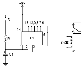
When activated by pressing a button, this time delay relay will activate a load after a specified amount of time. This time is adjustable to whatever you want simply by changing the value of a resistor and/or capacitor. The current capacity of the circuit is only limited by what kind of relay you decide to use.
Circuit diagram
Parts:
- C1 See Notes
- R1 See Notes
- D1 1N914 Diode
- U1 4011 CMOS NAND Gate IC
- K1 6V Relay
- S1 Normally Open Push Button Switch
- MISC Board, Wire, Socket For U1
Notes:
- Email jawaharlal@excite.com with comments, questions, etc.
- To calculate the time delay, use the equation R1 * C1 * 0.85=T, where R1 is the value of R1 in Ohms, C1 is the value of C1 in uF, and T is the time delay in seconds.
- S1 may be replaced with an NPN transistor so the circuit can be triggered by a computer, other circuits, etc.
- Most any 6V relay will work for K1. If you use a large relay, you my need to add a transistor to the output of the circuit in order to drive the larger load.
circuit from http://www.aaroncake.net/
