- Boost Your MP3 Power: 32 Ohm Amplifier Circuit
- Build Your 9V Bass Booster Circuit Diagram
- Build Your 20dB Audio Booster Circuit Diagram
- Symmetrical Class A Preamplifier – Build Your Audio Masterpiece
- Build Your Perfect Symmetrical 4 Channel Amplifier Circuit
- Build Your Ideal Buffer: Class A Circuit Diagram (560Ω)
- Discrete Preamplifier Circuit Diagram
- Build Your Own: Microphone Preamplifier Circuit (2mA)
- Stereo Preamplifier Circuit: Build Your +16dB Bass Boost
- Phono Preamplifier Circuit Diagram: 47K, 6.8K, 47nF Build!
- Modular Preamplifier Switching Center: Build Your Stereo Chain
- Portable Microphone Preamplifier Circuit Diagram – Build Your Own!
- Build Your Own Phono Preamplifier Circuit (18V)
- Amplify Signals: 741 Op-Amp Stethoscope Circuit Diagram
- Turn Speaker into Microphone: Build Your 6-12V Circuit
Build Your Perfect Symmetrical 4 Channel Amplifier Circuit
Description
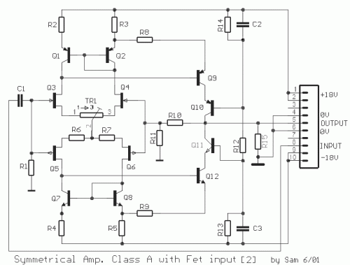
This is a balanced amplification unit circuit, characterized by a design that was initially conceived several years prior by Lisley Hood. The primary motivation behind this construction is to ensure the optimal selection of the field-effect transistor (FET) within a differential amplifier at the input stage. Despite this consideration, the circuit incorporates current mirroring stages on both sides, ultimately reducing the overall negative feedback effect. Precise matching of the transistors and their respective resistances are critical for optimal performance, and this is carefully addressed. The variable resistor TR1 mitigates any input offset voltage issues.
Circuit Diagram
Part List
- R1= 47Kohms
- R2-4= 220 ohms
- R3-5= 100 ohms
- R6-7= 470 ohms
- R8-9= 220 ohms
- R10= 5.6 Kohms
- R11= 1 Kohms
- R12= 10 Kohms
- R13-14= 820 ohms
- R15= 47 ohms
- TR1= 1 ohms trimmer
- C1= 4.7uF 100V MKT
- C2-3= 100nF 63V MKT
More about components
Several integrated circuits (ICs) are utilized within this circuit design. These components are crucial for providing specific functionalities and enhancing the overall performance of the amplifier. The BC214, BC212, BC182, BC184, 2N5457, 2N5460 are common NPN transistors integrated into the circuit. These transistors serve as switches and amplifiers within the circuit, contributing to its amplification capabilities. These ICs are selected for their robust characteristics, suitable for amplifying signals while maintaining stability and efficiency. The precise selection of these ICs is vital for achieving the desired amplification characteristics and minimizing signal distortion. The use of these ICs ensures the circuit operates reliably within the intended frequency range and maintains the required amplification factor.
