- Build a 4.7V USB Mobile Phone Charger Circuit
- Build Your 9V Ni-Cad Battery Charger Circuit
- Build Your Own NiCd Charger: 5V Circuit Design
- Build Your 5V USB Charger Circuit Today!
- Build Your 1.5V Pen Cell Mobile Charger Circuit
- Build Your Own 7.2V Mobile Charger Circuit
- Build a 3.6-6V Cellphone Charger Circuit
- Universal Battery Charger Circuit Diagram – Build Yours!
- Lithium-Polymer Peak Charger: Build Your 600mA Charging Circuit
- SLA Battery Charger Circuit: 2-Step Charging & Safety Features
- Battery Charger Regulator Circuit Diagram – 8V Design
- Build a Safe & Smart 5.6V Charger Circuit
- 12V Car Battery Charger: Build Your Constant Current Circuit
- Micropower Battery Protector Circuit Diagram for 4-10 Cell Batteries
- Build a Stunning Battery Status LED Flasher Circuit
SLA Battery Charger Circuit: 2-Step Charging & Safety Features
Description
This circuit was designed to supply power to a Peltier device within a vehicle. Power to the device originates from the vehicle's battery and is switched by a SPDT relay when the ignition is active, and from the SLA auxiliary battery when the ignition is deactivated.
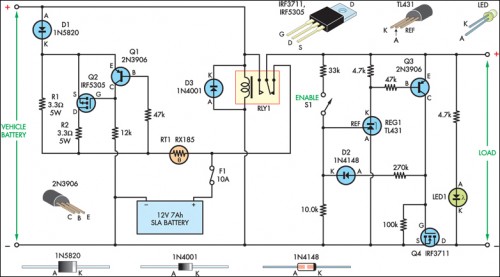
The SLA battery receives power from the vehicle's battery. During engine operation, the voltage remains remarkably stable, which greatly simplifies the charging circuit. If the SLA battery is fully charged, any additional charging current from the vehicle battery is limited by a 3.3W 5W resistor (R1). When the SLA battery is significantly depleted, the voltage across this resistor will be sufficient to activate PNP transistor Q1, subsequently turning on P-channel MOSFET Q2 and providing further charging current via R2 – essentially creating a two-stage charger.
Due to the parallel arrangement of resistors (R1 & R2), the combined voltage drop is reduced, resulting in a lower base bias for Q1, which in turn causes MOSFET Q2 to completely saturate. This positive feedback mechanism ensures a smooth transition between states and prevents Q2 from overheating due to partial conduction. The current then decreases gradually until the battery receives only a minimal charging current, and the voltage across the parallel resistors is only within the tens of millivolts. Schottky diode D1 prevents the SLA battery from discharging into the vehicle's accessory circuits when the engine is off.
Two safety components are integrated into the circuit: the initial in-line fuse F1 protects against severe damage in the event of shorts, and a PTC resettable thermistor (RT1) safeguards the battery from sustained over-currents during the charging phase. It is a 1.85A hold, 3.70A trip device at 23°C. Because it possesses a positive temperature coefficient, at 70°C, these ratings decrease to 1A and 2A for hold and trip, respectively, which further protects the battery.
Circuit diagram:
Finally, to protect the SLA battery from deep discharges, a low voltage disconnect is implemented. This system centers around REG1, a voltage reference configured as a comparator. Its reference (REF) input is connected to a voltage divider, provided that “enable” switch S1 is closed.
Whenever the voltage at REG1’s reference terminal exceeds 2.5V, its anode will be pulled low, biasing PNP transistor Q3. Q3 provides positive feedback through a 270kΩ resistor and diode D2 to activate N-channel MOSFET Q4, enabling power to be supplied to the load.
If the SLA battery voltage drops below 10V, the reference terminal will decrease below 2.5V, and the anode of REG1 will go high, removing bias from Q3 and turning off Q4 to disconnect the load and prevent deep discharge. LED1 indicates when power is being delivered to the load.
